IBM claims world’s first 2 nanometre data centre chip

As high performance computing (HPC) continues to demand higher performance and denser computing infrastructure, semiconductor manufacturers are locked in an increasingly intense fight to deliver breakthrough after breakthrough.
This week, IBM may have gained itself the upper hand over other chipmakers like Intel and NVIDIA. The company announced on Thursday that it has made a new breakthrough in semiconductor design, unveiling what it claims is the world’s first 2 nanometre (nm) node chip. To put that in persepctive, the smaller components of this chip are smaller than a single strand of DNA.

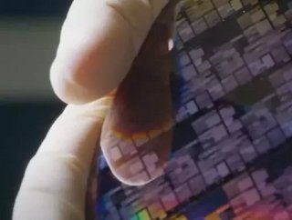
Close up on the individual switches in IBM's new 2nm chip - Courtesy of IBM
The potential benefits of the breakthrough could include quadrupling the battery life of cell phones - with IBM claiming that a smartphone using 2nm chip nodes would only require charging once every four days - drastically reducing the carbon footprint of data centres, and drastically boosting the performance of consumer electronics.
"The IBM innovation reflected in this new 2 nm chip is essential to the entire semiconductor and IT industry," said Darío Gil, SVP and Director of IBM Research. "It is the product of IBM's approach of taking on hard tech challenges and a demonstration of how breakthroughs can result from sustained investments and a collaborative R&D ecosystem approach."
IBM’s new nanosheet technology can apparently fit 50bn transistors onto a 150 mmsq chip.

That's a lot of transistors - Courtesy of IBM
Compared to 7nm chips currently on the market, IBM claims its 2nm designs are as much as 45% higher-performing, and use 75% less energy.
Whether this is actually the world’s “first” 2nm chip is actually something that is up for debate. As noted in Data Center Dynamics’ recent article, the ways in which different companies quantify node measurements has diverged in recent years, as nodes have become smaller and smaller.
This week’s announcement comes “less than four years” after IBM developed its prototype 5nm chip technology. However, it’s unlikely we’ll be seeing 2nm chips in smartphones any time soon, as IBM has yet to commercially launch its own 7nm chips. It plans to do so later this year.
It’s also entirely possible that 2nm is as small as chips will ever get. As semiconductors get smaller and smaller, the risk of electrons leaking from one part of the chip to another, even when its switches are off. In order to shrink its chips down to 2nm, Gil explained to Reuters that the IBM team was able to “drape sheets of insulating material just a few nanometers thick to stop leaks.”
He added: “In the end, there’s transistors, and everything else (in computing) relies on whether that transistor gets better or not. And it’s not a guarantee that there will be a transistor advance generation to generation anymore. So it’s a big deal every time we get a chance to say there will be another.”


