What Nokia's ATP Expansion Means for AI Infrastructure
Nokia has announced a major expansion of its advanced test and packaging (ATP) operations in Allentown, Pennsylvania, increasing domestic production capacity for the optical technologies that underpin modern data centres.
The investment is expected to increase manufacturing capacity at the site by up to ten times its current level, with new production coming online by the end of the third quarter.
The optical backbone of AI
As AI workloads grow in scale, the demands placed on data centre connectivity are increasing rapidly.
LLMs (large language models) and other advanced AI applications require vast amounts of data to move between compute clusters, storage systems and facilities with minimal latency.
That has placed greater importance on optical networking technologies, which provide the high-speed connections needed to support increasingly distributed AI environments.
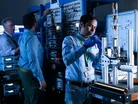
Nokia’s Allentown facility is one of only a small number of sites in the US capable of carrying out ATP processes for photonic chips.
These chips are integrated into optical modules that help move data across AI infrastructure and communications networks.
Justin Hotard, President and CEO of Nokia, said: “The AI supercycle is fundamentally reshaping network and infrastructure requirements in the US and globally.
“Our expansion in Allentown is a direct investment in that future – scaling domestic manufacturing of the optical networking technologies that power AI infrastructure.
“It also reflects the strong partnership between Nokia, the United States, and the Commonwealth of Pennsylvania to support advanced manufacturing, create jobs and strengthen US technology leadership and global competitiveness.”
The company says its optical networking technologies can reduce energy consumption in communications networks by as much as 75%.
Building capacity closer to home
The expansion is part of a wider effort to strengthen domestic semiconductor and photonics manufacturing.
Today, less than 2% of global semiconductor ATP activity takes place in the US.
By increasing local production of photonic components, Nokia aims to create a more resilient supply chain for the infrastructure supporting AI and digital services.
The project includes approximately US$30m of investment from Nokia.
It is being supported by around US$4m from the Commonwealth of Pennsylvania and approximately US$10m through the federal CHIPS investment tax credit.
Governor Josh Shapiro said: “Nokia is doubling down on the Lehigh Valley and ensuring that the future of chip production continues to run through this region because we’ve made smart investments to make Pennsylvania more competitive and proven that our Commonwealth is a great place to do business.
“As demand for semiconductors continues to grow across industries, we’ll continue to position Pennsylvania as a leader in innovation, with a supportive, thriving business climate that helps companies compete on a global scale.
“From advanced manufacturing to the research and development of new technology like advanced chip packaging, Pennsylvania has all the resources to be a world leader in chip production.”
Nokia also expects the expansion to nearly double its Pennsylvania workforce to more than 500 employees across engineering, manufacturing and research and development roles.

Supporting the next phase of AI growth
The investment forms part of Nokia’s broader multi-year plan to invest US$4bn in US research, development and manufacturing focused on AI-ready connectivity.
Bill Frauenhofer, Executive Director of Semiconductor Investment and Innovation at the Department of Commerce, said: “Nokia’s investment in Pennsylvania is directly advancing America’s AI leadership.
“Supported by CHIPS and Science Act funding, Nokia is deepening its commitment to innovation and the production of photonic chips in the United States.
“This project enables critical optical technology and strengthens America’s semiconductor supply chain.”
Company portals

Executives
Justin Hotard
President and CEO