What TSMC's Manufacturing Choice Means for AI Data Centres

TSMC has made a move that is set to influence the trajectory of chips powering AI data centres.
Taiwan Semiconductor Manufacturing Company (TSMC) has chosen not to adopt ASML’s latest High-NA EUV lithography machines for its A13 node.
As demand for AI and high performance computing continues to accelerate, decisions taken at the semiconductor manufacturing level are shaping how data centres scale capacity and efficiency.

What is TSMC’s A13 node designed to deliver?
TSMC’s A13 node, recently announced as a shrink of its A14 process, is designed to deliver improved density and efficiency.
These gains are critical for hyperscale data centres, where operators are under pressure to support more intensive AI workloads while managing power consumption and physical space.
Despite the high demand of AI data centres, TSMC has opted against integrating ASML’s new High-NA extreme ultraviolet (EUV) lithography into the A13 process.
Why is TSMC skipping High-NA EUV?
EUV lithography is used to print the most intricate layers on semiconductor wafers, enabling the production of smaller and more powerful chips.
High-NA EUV represents the next evolution, offering finer resolution but at significantly higher cost.
However, Co-Chief Operating Officer Kevin Zhang said the A13 node does not require the technology, according to reporting by Bloomberg.
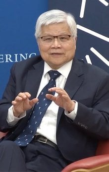
TSMC Chairman and CEO Dr CC Wei said of the A13 technology: “At TSMC, we understand our customers are always looking ahead to their next innovation and they come to us for a reliable stream of new silicon technologies, like A13, meticulously engineered to be ready for high-volume production right when their visionary new designs demand them.
“TSMC's advanced process technologies lead the industry in density, performance and power efficiency and we continually strive to make them even better for our customers' future products, ensuring customers' success as their most reliable technological partner.”
The A13 node is expected to support next-generation processors used in AI training and inference, as well as broader cloud and enterprise data centre environments.
Implications for the data centre supply chain
The market reaction to TSMC’s decision was immediate, with The Wall Street Journal reporting a 3% drop in ASML's shares, equivalent to US$16.76bn.
Despite this, the company remains Europe’s most valuable, with a market capitalisation of US$478.96bn.
The ripple effects extend across the data centre ecosystem. Semiconductor manufacturing decisions influence chip availability, pricing and performance, all of which affect how quickly operators can deploy new infrastructure.
A question of timing and strategy
TSMC’s choice not to adopt High-NA EUV at this stage raises questions about the timing of next-generation manufacturing technologies. Bloomberg reported the company may introduce the technology later in the decade, potentially around 2029.
This suggests that incremental improvements to existing processes will continue to underpin AI infrastructure growth in the near term.
At the same time, competitive dynamics remain in play. Other semiconductor manufacturers may choose to accelerate adoption of High-NA EUV in pursuit of differentiation,likely in AI-focused markets.
According to McKinsey, the semiconductor industry’s global value chain is under increasing strain from geopolitical tensions and supply constraints.
TSMC's decision signals that, even as AI demand surges, the path forward for data centre technology will be shaped as much by cost discipline and scalability as by raw innovation.
Company portals


Executives
C. C. Wei
CEO